


LVDS Interface Definition and Wiring Guide: Comprehensive Technical Manual
Author Introduction
This article is written by a senior embedded systems engineer with over 10 years of experience in industrial control, display equipment, and communication interface design. The author has led the development of multiple high-resolution display projects based on LVDS technology. This content combines theoretical knowledge with practical engineering experience to provide authoritative, professional, and practically oriented guidance for LVDS interface usage.
1. Introduction: Why Understand LVDS?
With the rapid growth of high-definition display requirements, traditional TTL (parallel) data transmission methods have exposed issues such as electromagnetic interference (EMI), complex wiring, and high power consumption at high speeds. Low Voltage Differential Signaling (LVDS) has emerged as a high-performance, low-power, and highly noise-immune data transmission technology widely used in LCD displays, industrial cameras, medical imaging devices, and automotive display systems.
Understanding the definition, electrical characteristics, and correct wiring methods of LVDS interfaces is crucial for electronic engineers, hardware designers, and even end-device maintainers.
2. Basic Definition and Working Principle of LVDS Interfaces
1. What is LVDS?
LVDS stands for Low Voltage Differential Signaling , a differential signal transmission technology that uses two lines (positive and negative pairs) to transmit complementary signals. The receiver extracts the voltage difference between the two lines using a differential amplifier to recover the original signal.
- Typical operating voltage : +2.5V to +3.3V
- Differential voltage swing : Approximately 350mV (typical value)
- Common-mode voltage range : 1.0V ~ 2.4V
- Transmission rate : Up to hundreds of Mbps to Gbps levels
2. Working Principle Overview
LVDS uses current-driven mode. At the transmitter, a constant current source generates approximately 3.5mA of current. This current switches direction across the two output lines according to the input logic level, forming a differential voltage. The receiver determines the logic state by comparing the voltage difference between the two lines.
This differential structure significantly enhances noise suppression capabilities, allowing LVDS to remain stable in long-distance and high-noise environments.
3. LVDS Interface Standards and Common Types
1. Common LVDS Interface Standards
| Standard Name | Application Area | Features |
|---|---|---|
| TIA/EIA-644-A | General LVDS Specification | Defines electrical characteristics, drive capability, and receive sensitivity |
| ANSI/TIA/EIA-899 | Multi-point LVDS (M-LVDS) | Supports multi-point bus topology |
| VESA DDI Standards | Display Interfaces | e.g., FPD-Link, LVDS Display Interface |
2. Common LVDS Interface Types
(1) Single Channel LVDS
Suitable for lower resolution display panels, typically includes:
- 1 clock signal (CLK)
- 3–4 data signals (DATA0–DATA3)
(2) Dual Channel LVDS
Supports higher resolution and refresh rates, often used for WXGA and above resolution LCD screens:
- Each channel has independent CLK and DATA lines
- Can be divided into Even/Odd or Upper/Lower modes
(3) Extended LVDS (OpenLDI)
Used in some high-end display devices, supports more data bits and more flexible timing configuration.
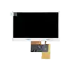
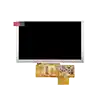
4. Physical Connection Methods of LVDS Interfaces
1. Interface Forms
Common physical forms of LVDS interfaces include:
- Ribbon cable sockets (e.g., JAE FX series, Hirose DF11)
- FPC flexible circuit board direct soldering
- Connector types : e.g., 30-pin, 40-pin, 50-pin LVDS sockets commonly used in laptops, industrial displays, etc.
⚠️ Note: Different manufacturers may define LVDS interfaces differently. Always refer to the device's specification sheet (Datasheet) for wiring.
2. Typical LVDS Interface Pinout (e.g., 30Pin)
| Pin Number | Signal Name | Type | Description |
|---|---|---|---|
| 1 | CLK_N | LVDS | Negative Clock |
| 2 | CLK_P | LVDS | Positive Clock |
| 3 | DATA0_N | LVDS | Data 0 Negative |
| 4 | DATA0_P | LVDS | Data 0 Positive |
| ... | ... | ... | ... |
| 29 | VCC | Power | Supplies backlight or other modules |
| 30 | GND | Ground | Ground connection |
Recommended Articles
-
Optimizing Human-Machine Interf
2025-05-29 -
Hangzhou LEEHON Technology Reco
2025-05-28 -
Report: Handheld Drone Ground C
2025-05-27 -
Report Title: Display Screen Se
2025-05-27 -
Downhole Operation Equipment Sc
2025-05-26 -
Optimizing Rail Transit Cockpit
2025-05-26 -
LCD Screen Selection and Soluti
2025-05-23 -
Optimizing Industrial Teach Pen
2025-05-23 -
How to Select a Screen for Ultr
2025-05-22 -
Optimal Infrared Display Select
2025-05-21 -
Machine Tool Control Panel Scre
2025-05-21 -
LCD Screen Selection Strategy a
2025-05-20 -
G057VN01 V2 LCD Panel for Cutti
2025-05-15 -
Why the Textile Industry Choos
2025-05-09 -
Outstanding Application and Adv
2025-04-28 -
Paperless Meeting System LCD Sc
2025-04-15 -
LEEHON's Comprehensive Screen S
2024-11-29 -
LEEHON's Comprehensive Screen S
2024-11-29 -
G104XVN01.0 as a Solution for W
2024-10-09 -
G190ETN01.4 and G150XTN06.0 as
2024-10-09